Ultra-thin kagome metal films could power next-generation electronics | Technology News
4 min readFeb 11, 2026 07:57 PM IST
In a fascinating step towards future electronic devices, scientists are now poised to harness an unconventional group of materials known as kagome metals. In a recent research paper, they claim to have synthesised an extremely thin type of antiferromagnetic material called iron germanide, which is composed of Fe and Ge.
However, the team, which was led by Chinese researchers from the State Key Laboratory of Semiconductor Physics and Chip Technologies, Beijing, has now found a method of creating high-quality FeGe (iron germanide) films on sapphire substrates made of aluminium oxide. Until now, most studies of this material relied on bulky single crystals. Creating it in thin, flat layers marks a major advance.
Why kagome materials matter
Kagome metals are named after a Japanese basket-weaving pattern that resembles their atomic structure. This geometric arrangement gives them unusual electronic and magnetic properties. In particular, FeGe exhibits both antiferromagnetism, in which adjacent magnetic moments point in opposite directions, and what appears to be a charge density wave effect, in which a pattern of electron configuration is established.
The development and possession of such properties make kagome materials vital in spintronics, which is an emerging technology used to control data based on spin instead of charge. The fact that kagome compounds behave in an antiferromagnetic manner is important since it enables an ability to operate quickly without any interference from magnets.
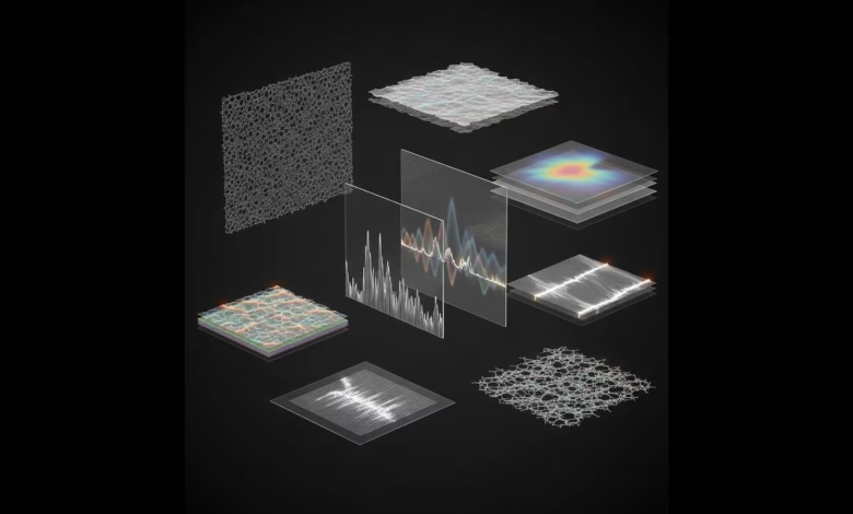
Grow the films layer by layer
They use a technique of thin film formation known as molecular beam epitaxy, where atoms can be placed in layers, and each can be placed individually. Three stages were part of the process. Firstly, a very thin iron or FeGe seed layer, only 2 nanometres thick, was deposited at high temperatures. The sample was then cooled quickly, and a thicker 15-nanometre FeGe layer was added at a lower temperature. Finally, the film was heated again for two hours to improve its crystal quality.
Tests using X-ray diffraction, atomic force microscopy, and high-resolution electron microscopy confirmed that the films were smooth and retained the distinctive kagome lattice structure. Adding a thin iron buffer layer significantly improved the surface flatness.
Strong magnetic order and a curious signal
Transport measurements showed that the films have a Néel temperature of 397 Kelvin, meaning they remain antiferromagnetic well above room temperature. This makes them practical for real-world devices.
Story continues below this ad
But one of the most interesting findings appeared around 100 Kelvin. Researchers observed changes in electrical resistance, Hall coefficient, and magnetoresistance behaviour that strongly suggest the presence of a charge density wave. Similar effects had previously been seen only in bulk FeGe crystals.
By analysing how resistivity changed with temperature, the team identified different scattering mechanisms at work, including interactions between electrons and vibrations in the lattice. Below 100 Kelvin, electron–electron interactions became particularly strong.
Toward next-generation spintronics
Producing FeGe as a thin film does more than confirm earlier findings. It allows scientists to manipulate the material using strain, electric fields, or even light—something much harder to achieve with bulk crystals.
Also Read: AI helps astronomers find 1,400 ‘Anomalous Objects’ buried in Hubble data
Story continues below this ad
Because the films are flat and compatible with standard semiconductor substrates, they could be integrated into electronic architectures. Their high Néel temperature and stable magnetic order make them strong candidates for future antiferromagnetic spintronic devices.
The researchers say further work will focus on understanding the charge density wave behaviour in greater detail. More advanced metal surface analysis equipment could explain the mechanism behind such electronic patterns.
For the time being, the capacity to produce good kagome layers of FeGe is an important breakthrough. While advancing the overall science of unusual quantum materials, it may also help to define the next stage of electronic innovation.
© IE Online Media Services Pvt Ltd


